Project Report For PCB & Mountings
Introduction
Project report for PCB Mountings is as follows.
A printed circuit board, or PCB, is the foundation of any electronic or electrical device. A PCB connects electronic components such as resistors, capacitors, coils, pots, diodes, FETs, transistors, ICs, transformers, and more to make a complete electronic circuit.
It is inconceivable to imagine any electrical equipment that exists today without a PCB. PCBs enable electronic equipment grow smaller and more efficient by enabling connectivity between electrical pieces.
Single layer PCBs and multi-layer PCBs are the two broad categories into which PCBs may be categorised. Electronic industries have a significant impact on almost every aspect of our everyday lives, including entertainment, communication, education, research and development, public services, defence, transportation, agriculture, and health care.
The electronic sector is expanding at a very rapid rate due to the rising demand for electronic equipment and gadgets in every aspect of human life.
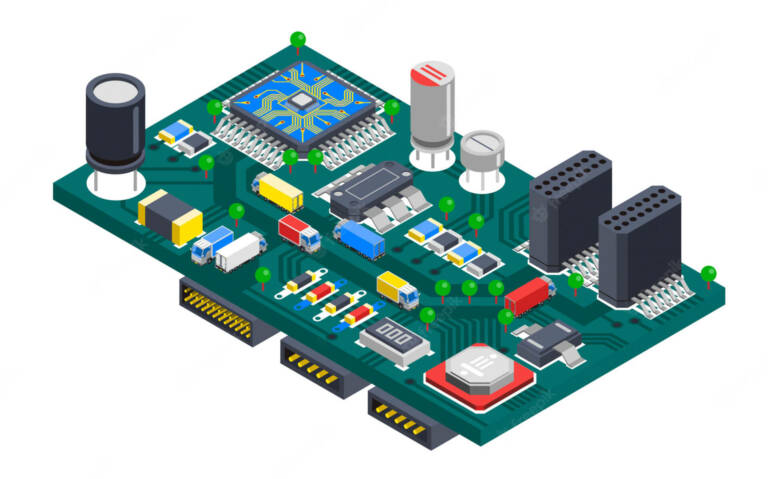
Micro service industries, such as mounting/assembling electronic components on PCBs, are becoming more and more in demand to meet the needs of small, medium, and large size electronic companies. For the PCB assembly of lead-filled electronic components, a project profile has been developed. PCBs and componentry are provided by the customer.
Product & Application of PCB & Mountings
Electronic components are mechanically supported by printed circuit boards, or PCBs, by having their connection leads soldered onto copper pads for surface mount applications or through drilled holes in the board and copper pads for soldering the component leads for thru-hole applications.
A board design may feature surface mount components on both the top and bottom of the board, all thru-hole components on the top or component side, a combination of thru-hole and surface mount components on the top side and surface mount components on the bottom or circuit side.
Additionally, conductive copper traces are used on the boards to electrically connect the necessary leads for every component. Copper sheets bonded over a non-conductive substrate are used to create the component pads and connection traces.
Single-sided printed circuit boards have copper pads and traces on just one side of the board, double-sided boards have copper pads and traces on the top and bottom sides, and multilayer boards have copper pads and traces on the top and bottom of the board as well as a variable number of internal copper layers with traces and connections.
Get Completely Custom Bankable Project Report
The project’s promoter may have any type of degree in addition to training or expertise in electronics or electrical maintenance.
Market Potential Of PCB Mountings
The size of the worldwide printed circuit board industry, which was estimated to be worth USD 78 billion in 2021, is predicted to grow to USD 128 billion by 2030, showing a CAGR of 5.66% from 2022 to 2030.
Expenses

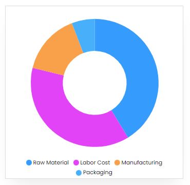
Product Cost Breakup
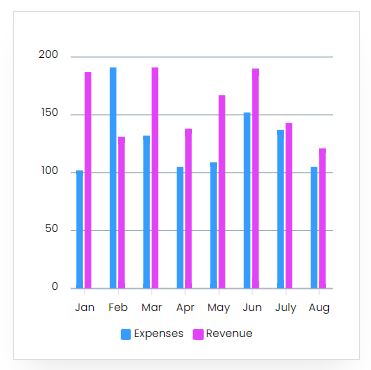
Reveneue Vs Expenses
Market Trend

In all electronic and the majority of electrical equipment, PCBs are used. Without a PCB, it is impossible to understand how any electronic device would function, including home appliances, entertainment equipment, testing devices, medical devices, and even devices used in the military.
Numerous vendors are available to the small, medium, and big size units to do the particular task. Another ancillary task is putting electronic components on PCBs. The cost of this kind of work is determined on the size and complexity of the PCB. The testing tools and raw materials needed to run this kind of service unit are readily available locally.
Market Analysis Of PCB Mountings
The Indian printed circuit board (PCB) market is primarily driven by the region’s thriving consumer electronics sector, which is predicted to grow rapidly in the coming years. Sales of computers, cell phones, and tablets are expanding in India, owing to increased urbanization, rising living standards, and rising disposable incomes of the majority of the population, and PCBs are an essential component of their mechanism.
This is bolstered further by the Government of India’s proactive measures to boost indigenous consumer electronics manufacturing facilities. Many programs, including ‘Made in India,’ ‘Digital India,’ and the National Policy on Electronics, have resulted in significant growth in domestic demand for PCBs.
Furthermore, the growing trend of computer miniaturization is boosting the market growth. Manufacturers limit the size of semiconductor devices not just to lower the size of electronics and make them more aesthetically pleasing, but also to improve their overall performance.
It, in conjunction with the introduction of numerous innovations in the way of generating PCBs, offers impetus to the market’s development. The increasing use of digitalization and modernization in the medical sector is also predicted to have an impact on PCB demand in the future years, resulting in a positive market forecast.

